How to Reduce Latency in VLSI
Latency is a significant concern in the world of Very Large Scale Integration (VLSI) design. It refers to the delay between the initiation of a process and its completion. High latency can impact the overall performance of electronic devices, leading to slower processing speeds and decreased efficiency.
Reducing latency in VLSI is crucial for ensuring optimal performance and efficiency. In this article, we will explore some strategies to minimize latency in VLSI design.
1. Minimize Wire Length
One of the primary causes of latency in VLSI design is the length of the wires connecting various components. Longer wires result in increased resistance and capacitance, leading to higher latency. By designing layouts that minimize wire length, designers can reduce latency and improve overall performance.
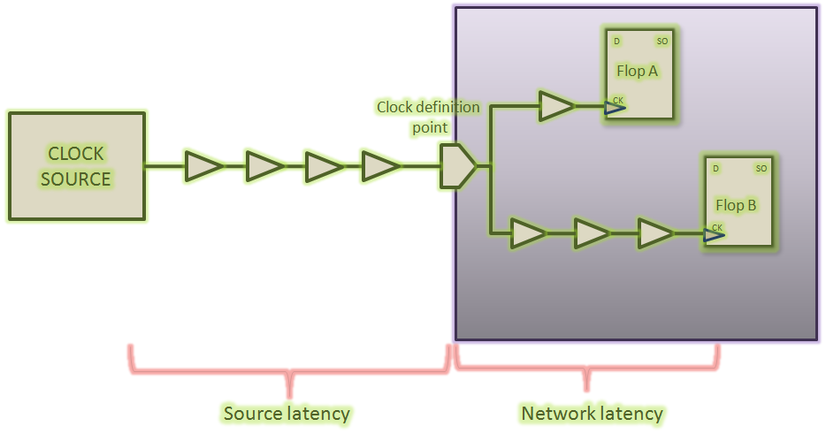
2. Optimize Clock Distribution
Efficient clock distribution is essential for reducing latency in VLSI circuits. Clock signals must be distributed evenly and accurately to all components to ensure synchronous operation. By optimizing clock distribution networks, designers can minimize clock skew and reduce latency in the system.
3. Implement Pipelining
Pipelining is a technique used to break down complex processes into smaller stages, allowing for parallel processing and reduced latency. By implementing pipelining in VLSI design, designers can improve performance and efficiency by overlapping the execution of multiple instructions.
4. Use High-Speed Interconnects
High-speed interconnects, such as high-speed buses and interconnect protocols, can help reduce latency in VLSI circuits. By using high-speed interconnects, designers can ensure faster data transmission and communication between components, resulting in lower latency and improved performance.
5. Optimize Power Delivery
Efficient power delivery is crucial for reducing latency in VLSI circuits. Inadequate power distribution can lead to voltage drops and signal integrity issues, resulting in increased latency. By optimizing power delivery networks and minimizing voltage drops, designers can improve performance and reduce latency in VLSI designs.
6. Utilize Advanced Design Tools
Utilizing advanced design tools and methodologies can help designers optimize VLSI designs for reduced latency. Tools such as static timing analysis, layout optimization, and simulation tools can aid in identifying and addressing potential latency issues early in the design process, improving overall performance and efficiency.
7. Conduct Detailed Timing Analysis
Conducting detailed timing analysis is essential for identifying and mitigating latency issues in VLSI designs. By analyzing signal paths, clock domains, and critical paths, designers can pinpoint areas of high latency and implement targeted optimizations to reduce latency and improve overall performance.
8. Implement Design-for-Testability Techniques
Design-for-testability techniques can help designers reduce latency by simplifying the testing and debugging process. By incorporating test structures, scan chains, and built-in self-test (BIST) circuits into VLSI designs, designers can quickly identify and resolve latency issues during testing, leading to improved overall performance.
In conclusion, reducing latency in VLSI design is crucial for ensuring optimal performance and efficiency. By implementing strategies such as minimizing wire length, optimizing clock distribution, and using high-speed interconnects, designers can significantly reduce latency and improve overall performance in VLSI circuits.